| Telephone: | 86-15148215714 |
| E-MAIL : | yang_fan@forsense.cn |
| Position : | Room 4F,Building 16,No. 1000 JinhaiRoad, City of Elite,,Pudong New Area,Shanghai |
 |  |  |  |
| Sample purchase |
Oblique Plot FSS-IMU614E-P
IMU614E-P inertial module can achieve low cost, high precision and anti-magnetic interference attitude measurement and orientation through data fusion algorithm of IMU and GNSS. Especially in the field of RTK oblique mapping, accurate and consistent oblique position correction can be achieved.
For surveying and mapping poles, it provides ±2.5cm measuring accuracy in the range of_30° inclination Angle, and has the function of correcting installation deviation Angle, which can be adapted to all kinds of centering poles.
1.Key indicators of Gyroscope
| Parameters | Test Conditions / Remarks | Typ. | Unit |
| Measurement Range | ±500 | °/s | |
| Bias instability | @25℃, Allan Variance, 1σ | XY: 5.0 Z: 4.0 | °/hr |
| Misalignment | 0.01 | deg | |
Internal Low-pass Cutoff Frequency | Adjustable Software | 47 | Hz |
| ODR | 1000 | Hz | |
| Measure Delay | 5.0 | ms | |
Offset Error over Temperature | -40℃~85℃, ≤1℃/min@1σ | 0.01 | °/s |
| Random Walk | @25℃, Allan Variance, 1σ | 0.3 | °/√hr |
| Scale Coefficient Error | 1.0 | ‰ | |
| Scale Factor Nonlinear | 200 | ppm |
2.Key indicators of Accelerometer
| Parameters | Test Conditions / Remarks | Typ. | Unit |
| Measurement Range | ±6 | g | |
| Bias instability | @25℃, Allan Variance, 1σ | 25 | μg |
| Misalignment | 0.01 | deg | |
| Internal Low-pass Cutoff Frequency | Adjustable Software | 47 | Hz |
| ODR | 1000 | Hz | |
| Measure Delay | 5 | ms | |
| Offset Error over Temperature | -40℃~85℃, ≤1℃/min@1σ | 0.1 | mg |
| Random Walk | @25℃, Allan Variance, 1σ | 0.05 | m/s/√hr |
Scale Coefficient Error | 3.0 | ‰ | |
| Scale Factor Nonlinear | 200 | ppm |
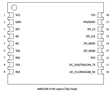
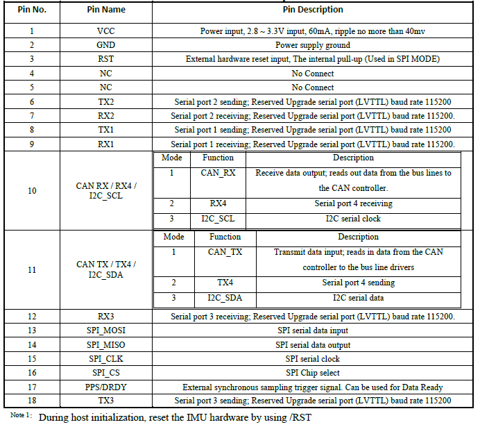
3.Pin Defination

Pin No. | Pin Name | Pin Description | ||
1 | VCC | Power input,+3.3V input,40mA,ripple no morew than ±40mV | ||
2 | GND | Power supply ground | ||
3 | RST 1 | External hardware reset input, Theinternal pull-up (Used in SPI MODE) | ||
4 | NC | No Connect | ||
5 | NC | No Connect | ||
6 | TX2 | Receive asynchronous data output | ||
7 | RX2 | Receive asynchronous data input | ||
8 | TX1 | Receive asynchronous data output (Data communication interface (LVTTL)) | ||
9 | RX1 | Receive asynchronous data input (data communication interface (LVTTL)) | ||
10 | CAN RX / RX4 / I2C_SCL | Mode | Function | Description |
1 | CAN_RX | CAN Receive Pins; Reads data from the bus to the CAN controller | ||
2 | RX4 | Receive asynchronous data input | ||
3 | I2C_SCL | I2C serial clock | ||
11 | CAN TX / TX4 / I2C_SDA | Mode | Function | Description |
1 | CAN_TX | CAN transmit pin; Reads data from the CAN controller to the bus driver | ||
2 | TX4 | Receive asynchronous data output | ||
3 | I2C_SDA | I2C serial data | ||
12 | RX3 | Receive asynchronous data input | ||
13 | SPI_MOSI | SPI Serial Data Input | ||
14 | SPI_MISO | SPI Serial Data Output | ||
15 | SPI_CLK | SPI Serial Clock | ||
16 | SPI_CS | SPI chip select | ||
17 | PPS | External synchronous sampling trigger signal; (Access to RTK second pulse pin) | ||
18 | TX3/DRDY | Receive asynchronous data output/can be used for Data Ready | ||
Note1:During host initiallization, reset the IMU hardware by using /RST
4. Electrical Characteristics
Parameter | Symbol | Scope | Units |
Power input | VCC | -0.3 to 4 | V |
Power GND | GND | - | - |
Input Pin Voltage | Vin | -0.3 to VCC+0.2 | V |
Operating Temperature | Tot | -40 to 85 | ℃ |
Storage temperature | Tstg | -40 to 85 | ℃ |
1.External Structure
Outline Structure and Dimensions (unit: mm)


2. Pin Description

3. PCB Pad Size Drawing


